Building Your Own Trezor Hardware Wallet - Part 3
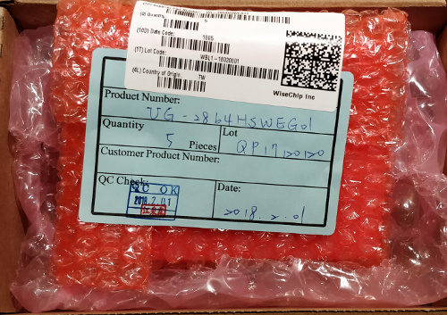
The OLED displays finally arrived! Turns out that futureelectronics.com took about three weeks from placing an order to actually shipping the package out. Once shipped it arrived in reasonable time though.
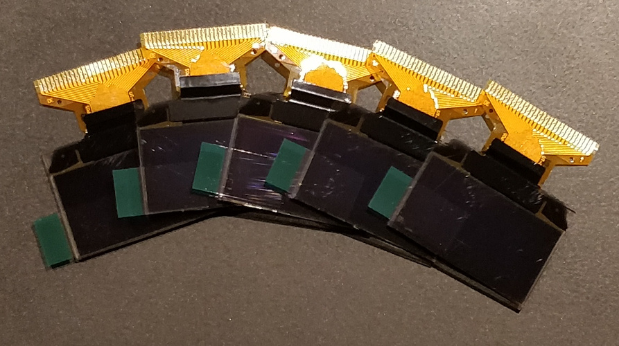
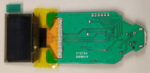
OLED display assembly
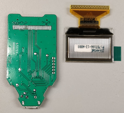
Now to finally finish assembling the board! First thing to do when soldering on the OLED display would be to apply some solder flux and tin the pads on the PCB.
Alignment
Next, line up the flat flex cable with the pads.
Make sure that you do not put the OLED display on backwards! The flat flex cable is meant to wrap around from the back of the PCB to the front. Attaching the OLED display backwards will result in incorrect pin connections and could cause damage to the display or to the microcontroller if the board is powered on.
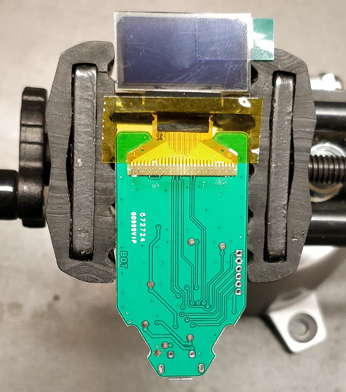
The alignment must be quite precise and the contacts on the flat flex should cover the pads on the PCB completely. If the board was designed correctly then the pads will be same size as the flat flex contacts. There should not be any exposed part of the pads showing if the flat flex is aligned correctly. Secure the flat flex assembly to the PCB with some kapton tape, or any other kind of tape which won’t leave much of a reside and is at least somewhat heat resistant.
It is also a good idea to secure the whole assembly using something such as a small vice.
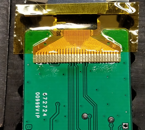
You might notice that the flat flex contacts have small holes in them. This is to allow solder to flow up through rather than to the side where the other contacts are which helps prevent unwanted solder bridges.
Soldering
With the pads on the PCB pre-tinned, all that should be required is to heat up each of the flat flex contacts with a soldering iron. The solder on the pads should melt and flow up through the holes in the flat flex. You’ll know when it is done once the flat flex contacts change from their copper colour to a shiny silver colour of the solder. After the solder has cooled, the tape can be carefully removed.
Acquiring the bootloader binary
To get the flashable firmware binaries, there are two routes you could take:
- Build the Trezor firmware from source found on the official Trezor firmware Github repository. Instructions can be found on the README.
- Download the pre-compiled and signed firmware binaries from wallet.trezor.io. Instructions can be found on the same README file.
Only the bootloader bin file is actually necessary, the main Trezor firmware can be flashed on after using the standard Trezor wallet browser app. The bootloader needs to be flashed manually so that the Trezor wallet app recognizes the hardware as a Trezor and so that the hardware can actually boot something!
Flashing the bootloader
With the board fully assembled, the microcontroller needs a bootloader flashed onto it. When buying an microcontroller straight from an electronics supplier, the on-board flash memory is completely blank with no bootloader or firmware at all.
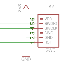
SWD header
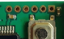
The six small holes on the left side of the board are the SWD header for the Atmel microcontroller. The pinout of this SWD header can be determined by referencing the schematic for the Trezor hardware.
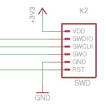
On the schematic this header has the designator K2 as well as the label “SWD”. On the physical board, pin 1 is indicated by the square pad where as all the other pads are circular.
Pin 1 is not indicated on the schematic, but another trick is to inspect the physical traces on the PCB to see where they lead to. It is quite clear that pin 2 is connected to the large plane on the top of the board, and that this is most likely a ground plane. Pin 6 goes to a wide trace and connects to pin X of the microcontroller. There is also a capacitor between this wide trace and the suspected ground plane. This wide trace must be a positive voltage (VDD) net; on this board the only voltage net is the +3.3V power net. Therefore, pin 1 of the K2 header on the schematic must be the bottom most pin.
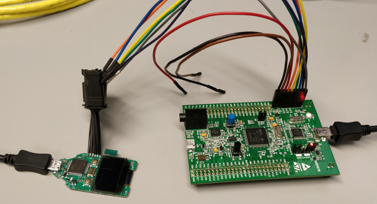
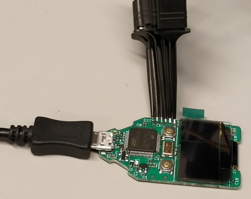
Connecting a programmer
A programmer capable of flashing an STM32 microcontroller is required. For this I used an STM32F4 Discovery development board because it has a on-board ST-LINK/V2 programmer which can be configured as standalone to program and debug external STM32 boards (I also had one laying around already). It is just a matter of connecting up the SWD connector of the ST-LINK/V2 to the SWD header on the Trezor PCB by matching up pin names.
Since this will be temporary and a one-time thing, I used some small test hook clips to connect to the SWD header and then used some female-to-female 0.1” header wires to connect the other end to the ST-LINK/V2 SWD connector. These proved to be a bit tricky to ensure that there was good contact between the through-hole pads and the test hooks, but once I found a position where all six were in good contact, I left it on the desk being careful not to bump it or else I might have to adjust it all again.
Flashing
The ST-LINK utility software can be used to flash on a fresh bootloader. This is officially supported software for the ST-LINK/V2 provided by ST themselves. Annoyingly, you must provide a valid email address in order to get the download link for the software (why do companies think that forcing people to do this is a good idea?).
Unfortunately I did not take any screen shots of the ST-LINK utility software during the process. The software is easy enough to use though.
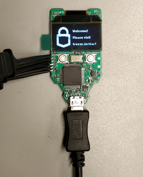
Finale
It works!
With the bootloader flashed, the initial Trezor welcome screen is shown on the OLED display. Pushing each of the two momentary buttons will cause a small square on the display. This can be used to confirm that the microcontroller can read button presses and that the electrical contacts are good.